
NEW DELHI, August 17, 2026, 08:39 IST
- India now has three semiconductor plants in commercial production.
- All three operating sites assemble, package or test chips made from imported wafers.
- India’s first front-end silicon fab is scheduled to start in 2028.
India has moved from semiconductor plans to commercial output at three plants. Prime Minister Narendra Modi said exports have also begun from the sites. He expects five to eight more facilities within seven to eight years.
The milestone is real, but narrow. Each operating plant handles assembly, packaging or testing. None makes silicon wafers from scratch.
That distinction matters for phones, cars and AI servers. Packaging adds meaningful value and creates a qualified supply base. Front-end fabrication remains the harder test of India’s manufacturing strategy.
Micron Technology (NASDAQ:MU), Kaynes Technology India (NSE:KAYNES) and CG Power and Industrial Solutions (NSE:CGPOWER) anchor the first operating wave. Their disclosed scale differs sharply.
| Operating site | Commercial start | Work performed | Disclosed investment | Disclosed output |
|---|---|---|---|---|
| Micron, Sanand | February 28, 2026 | DRAM and NAND assembly and test | About $2.75 billion, including government support | Tens of millions of chips in 2026; hundreds of millions in 2027 |
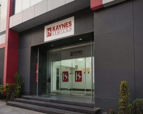
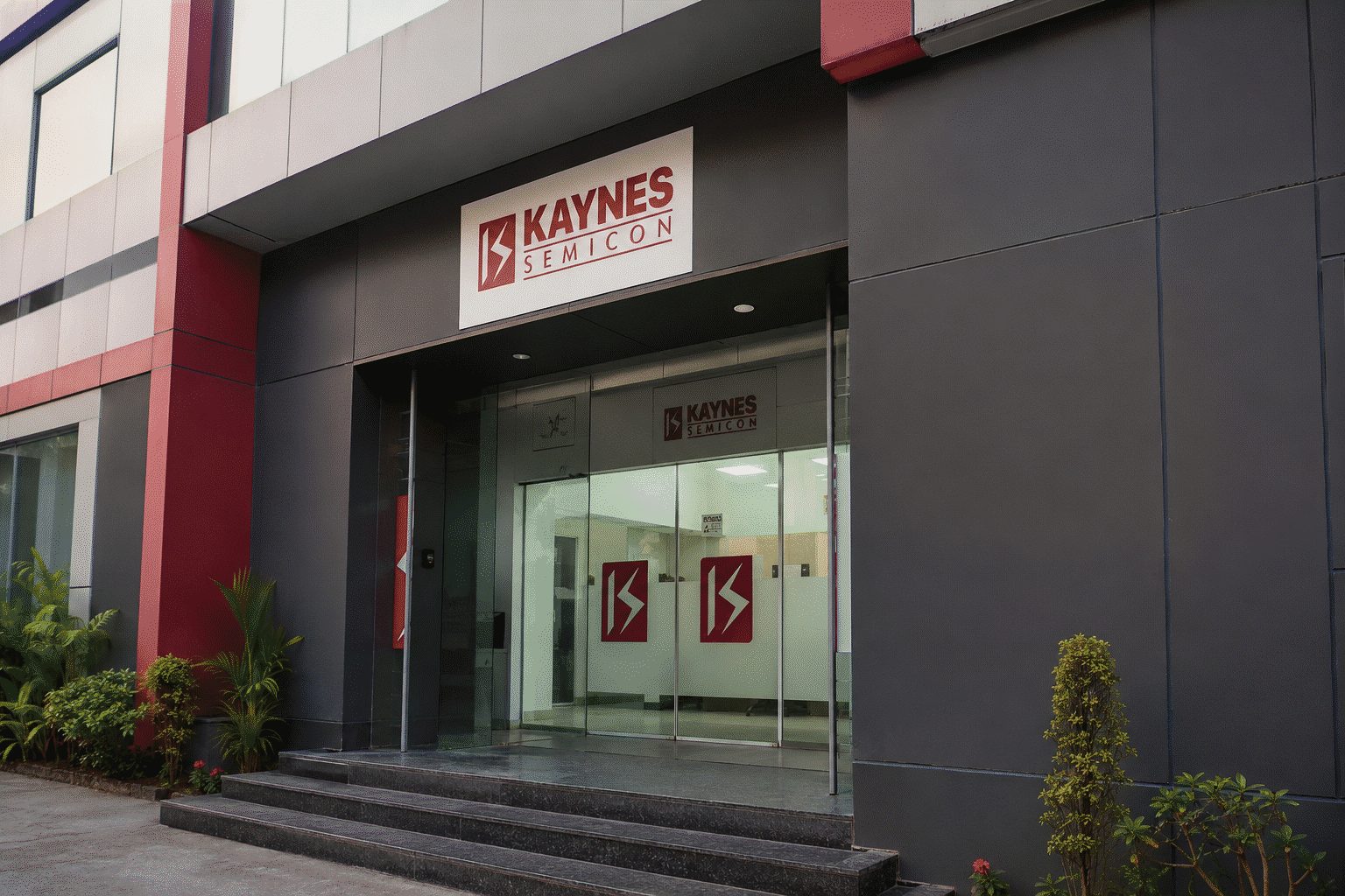
| Kaynes Semicon, Sanand | March 31, 2026 | OSAT, including intelligent power modules | ₹3,300 crore | Approved capacity: 6 million chips per day |
| CG Semi, Sanand | July 4, 2026 | OSAT for consumer, industrial, automotive and power uses | ₹7,600 crore | 200 million annually at launch; target of 5 billion annually |
Micron says its Sanand plant converts DRAM and NAND wafers from its global network. The company expects hundreds of millions of finished chips there next year.
Kaynes began production on March 31. CG Semi followed on July 4. Government records place their approved daily capacity at 6 million and 15 million chips, respectively.
| Approved unit type | Number | Role in the value chain | Current verified status |
|---|---|---|---|
| Silicon fab | 1 | Front-end wafer fabrication | First commissioning scheduled for 2028 |
| Silicon-carbide fab | 1 | Compound-semiconductor fabrication | Approved; commercial start not disclosed |
| Integrated GaN and micro-LED display fab | 1 | Compound semiconductors and displays | Approved; commercial start not disclosed |
| Packaging units | 9 | Assembly, marking, packaging and test | Three operating; one more expected in 2026 |
The government has approved 12 plants with investment above ₹1.64 lakh crore. Nine are packaging units. The mix shows where India can enter the supply chain fastest.
| Program | Budget outlay | Verified progress | Central industrial challenge |
|---|---|---|---|
| Semicon 1.0 | ₹76,000 crore | 12 manufacturing units approved; three packaging plants operating | Turn approved fabs into qualified, repeatable production |
| Semicon 2.0 | ₹127,500 crore | Approved July 15, 2026; six policy pillars defined | Build design IP, equipment, materials, advanced nodes and talent |
The first silicon fab is Tata Electronics’ planned Dholera plant. It uses a 300-millimetre platform and targets automotive, mobile and AI chips. ASML Holding (AMS:ASML) agreed in May to support the project.
Semicon 2.0 makes that gap explicit. Its six pillars cover design, machinery, materials, fabs, packaging, research and talent. The government says the first silicon fab will be commissioned in 2028.
“The entire value chain should be ours,” Modi said in his Independence Day address. That goal now has operating proof at the packaging stage. It does not yet have front-end proof.
Risks: The new plants still depend on overseas wafer supply, equipment and materials. Large fabs also face execution, yield, customer-qualification and demand risks.
For buyers, near-term effects will be indirect. More packaging capacity can diversify supply and shorten some routes. Pricing benefits depend on volume, yields and long-term customer contracts.